 Delete Article!
-
222009. 07
No. 24 View. 5765
KAIST develops core technology for world's first surface plasmon OLED
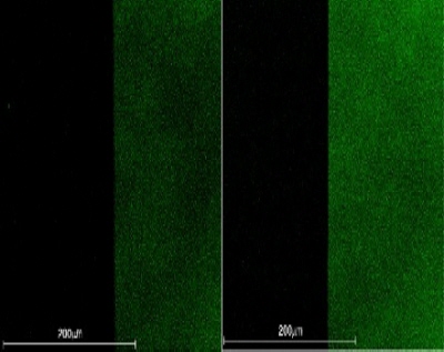
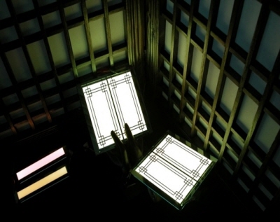
Prof. Choi Kyung-chol team's technology to allow for low-cost, normal temperature OLED processing.The Korea Advanced Institute of Technology (President Suh Nam-pyo) said on July 9 that a research team led by Prof. Choi Kyung-chol at the institute's electrical and electronic engineering department had become the first in the world to develop a core technology that significantly enhances the efficiency of OLEDs, an electronic display device. Prof. Choi's team discovered that when a material inducing surface plasmon is combined with light generated from an OLED using nano-size silver (Ag) particles, the speed at which light emission recombines increases, thus significantly enhancing the brightness of the OLED. Additionally, the team increased the efficiency of light emission by up to 75 percent by allowing for low-cost, normal temperature OLED processing using surface plasmons through the application of an evaporation method for the first time in the world. (Photo) A photo of OLED light emission using surface plasmons compared with a photo of that light emission in a conventionally structured OLED. The study is drawing keen attention for inventing a new display device that combines OLED, a next-generation display technology, with surface plasmon technology using low-cost nanoparticles.Prof. Choi said, "The technology that has been developed using surface plasmons is a new technology that can enhance the emission efficiency of OLEDs," adding, "The technology is expected to make important contributions to the acquisition of core technology and to the development of OLED and flexible display technology." The study was published in Applied Physics Letters, a world-renowned journal in the applied physics field, and Optics Express, the most prestigious journal in the optics field. The study was conducted with support from the "Frontier research center program" of the Korea Research Foundation (Chairman Park Chan-mo), and from the "KAIST high risk, high return program" at the Nanopap Center (President Lee Hee-chul).Yoo Sang-young, young at hellodd.com [July 21, 2009] - - - - - - -Source - HelloDD.com -
222009. 07
No. 23 View. 6676
KIMS secures technology for highly porous, sturdier ceramic
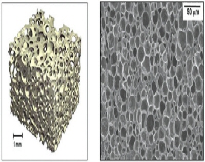
Efforts kick off to commercialize core technology for microcellular, porous ceramic? (Photo) Efforts are underway to commercialize a state-of-the-art core technology that allows for the creation of invisible holes in ceramic materials but minimizes the deterioration of the mechanical functions of such materials.A team led by Dr. Song In-hyuk of the engineering ceramics research group at the Korea Institute of Materials Science (Director Cho Kyung-mok) said on July 13 that, working with a research team led by Dr. Kim Young-wook at the University of Seoul, it jointly developed a core technology for microcellular, porous ceramic, a material for which pore control is of utmost importance.Song's team is jointly conducting research with Youngjin Ceramics (CEO Bae Ji-soo) and Namkang Ceramics (CEO Yoon Dal-woong) to commercialize the technology and transfer related technologies. Notably, Youngjin Ceramics successfully produced a setter (a structure that maintains its electrical characteristics when forming ceramic products, including electronic parts and porcelain) comprising diverse formations based on the core technology.Dr. Song said, "By applying microcellular, porous ceramic technology, and thus reducing the weight of ceramics through the presence of numerous pores, we can produce components that can enhance efficiency in heat treatment when forming, and that are consistent in composition thanks to convenient degreasing on the contact surface at the bottom resulting from enhanced porousness."With the adoption of the technology, the porous Zirconia setter is expected to cut materials costs of a product by 40 percent and production costs by 20 percent, allowing producers to rake in 1.5 billion won in annual sales.Dr. Song said, "We have conducted research since 2001, and initially focused on the acquisition of core technology, including the development of new processes," adding, "Through proactive research collaboration with companies, we aim to commercialize in the short-term strategic items, including vacuum chuck materials that can be applied to semiconductor equipment and LCD equipment, which require a high level of porousness, and a light tile material that allows for humidity control as an eco-friendly construction material."Additionally, Dr. Song's team and Youngjin Ceramics are expanding the applicability of the technology by producing porous Zirconia setters and a brush for polishing printed circuit boards. As such, experts predict the technology will highly likely find applications in other fields in the future.Dr. Song said, "The microcellular, porous ceramics technology will emerge as a technology for creating core materials that overcome technological barriers in the areas of the environment, precision machinery, automobiles, construction materials, medical components and fuel cell projects."Amid increasing international concern for environmental matters, porous materials are catching on around the world in the fields of desulphurization, denitrification, and filters aimed at curbing environmental pollution. As such, the utility and value of microcellular ceramics that boast functional superiority over conventional porous materials will likely increase further.The applicability of the technology is also expected to expand to include semiconductors, heat-resistant tiles for space shuttles, high pressure ramps, and artificial bones and joints.Lim Eun-hee,redant645 at hellodd.com[July 21, 2009]- - - - - - -Source - HelloDD.com -
202009. 07
No. 22 View. 5850
1st Joint Workshop for Collaboration between KISTI and IPNS/KEK
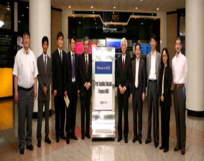
KISTI has hosted "1st Joint Workshop for collaboration between KISTI and IPNS/KEK" on July 17 at its head office located in Daejeon. The workshop has been organized in cooperation with KEK, which is a high-energy physics research organization in Tsukuba, Ibaraki Prefecture, Japan. This workshop aimed to lay the foundation for an active information exchanges to promote joint research on electron-positron colliding-beam accelerator. The event began with a talk between Trustee of KEK, Dr. Fumihiko Takasaki, and President of KISTI, Dr. Park Young-seo, and proceded with the participants' presentations and discussions on the current state of each organization and future collaboration such as plans for promoting the exchange of technology between KISTI and KEK. -
082009. 07
No. 21 View. 5659
The First Minister of S and T Visits KISTI
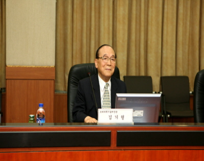
The First Minister of Science and Technology, Kim Ki-hyung, made a visit to Korea Institute of Science and Technology Information(KISTI, President Park Young-seo) on July 7. The event began with a talk between the First Minister Kim and KISTI staffs including President of KISTI, Park Young-seo, and was followed by an introduction to KISTI and a tour of its facilities. During the visit, he showed considerable interest in KISTI's research activities and also encouraged KISTI staffs. -
292009. 06
No. 20 View. 4484

KISTI hosts a conference "The Clouds 2009"
'K-cloud' makes a startConference "The Clouds 2009" on July 8 - Discussion on standardization policy Korea Institute of Science and Technology Information(KISTI, President Park Young-seo) will hold a conference "The Clouds 2009" in cooperation with Korea Cloud Service Association, Korea IT Service Industry Association, Cloud Computing Forum, and The Electronic Times at the COEX Intercontinental Hotel Seoul on July 8. The conference's aim is to gather, analyze and propagate the technological information related with Cloud Computing, research and analyze the latency information of Cloud Computing and support new policy for Government as well. More than 500 attendants include computing analysts and participants interested in cloud service. The sailing ceremony of 'Cloud Computing Forum' will also be held as the first step of K-cloud on the same day. This forum, in which KISTI and Association of Next Generation computing Industry, and others are participated, plans to conduct standardization policy researches on Cloud Computing. Cloud Computing is one of the most promising IT concepts, which is when users run software over the internet and access it via a browser. It is a style of computing in which dynamically scalable and often virtualized resources are provided as a service over the Internet.The term cloud is used as a metaphor for the Internet, based on how the Internet is depicted in computer network diagrams and is an abstraction for the complex infrastructure it conceals. -
262009. 06
No. 19 View. 5520
KAIST develops conducting nanowire
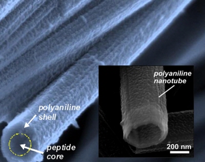
Prof. Park Chan-beum's team uses peptide self-assembly tech, publishes study in international journal. (Photo) Image of vertically well-aligned nanowire and nanotube.A team of Korean researchers has developed conducting polymer nanowire and nanotube material that employ natural peptide self-assembly technology. The Korea Advanced Institute of Science and Technology (President Suh Nam-pyo) said on June 15 that a team led by Prof. Park Chan-beum at KAIST's department of materials science and researcher Ryu Jung-ki had published their study on the development of conducting polymer nanowire and nanotube material in Angewandte Chemie, a world-renowned chemistry journal. Peptides or proteins can create three-dimensional structures through the combination of some 20 amino acids. Such structures have the advantage of outstanding physical characters and diverse functions, which were not available in the original materials. The research team allowed tens of thousands of very simple peptides comprising two amino acids to align on their own to successfully form a long nanowire one one-thousandth the thickness of a single hair. They then coated the structure with polyaniline, a conducting polymer material, to create a Vertically Well-Aligned conducting Nanowire. Unlike common electric wires, the Vertically Well-Aligned nanowire only conducts electricity on its surface. Prof. Park's team then selectively removed the peptide core section of the conducting nanowire to produce a conducting nanotube consisting purely of polyaniline.Creating three-dimensional structures through the self-assembly of chemical substances, a process not unlike building with Lego blocks, not only constitutes a fundamental mechanism within all different biological phenomena, but is also widely sought after as one of the key technologies for producing nanomaterials. Notably, since the peptide the research team used in the study originated from amyloid plaque in a fabric structure, which is closely related with the development of degenerative diseases including Alzheimer's, the study of the self-assembly of peptides is highly important from a medical perspective as well. If conducting polymer is produced into a nano-sized structure, its electric characteristic is significantly enhanced. Hence, the newly developed conducting nanowire and nanotube will likely find applications in the development of various next-generation solar cells, sensors and chips, and are expected to help boost Korea's science and technology competitiveness in the areas of nano-bio fusion in the future.Meanwhile, experts say the newly developed technology has already made important contributions to the development of nanomaterials through the creative fusion of nanotechnology and bioscience.Lim Eun-heeredant645 at Hellodd.com(Photo) From left: Prof. Park Chan-beum and Ph.D. candidate Ryu Jung-ki, researcher[June 26, 2009]- - - - - - -Source - HelloDD.com -
222009. 06
No. 18 View. 5436
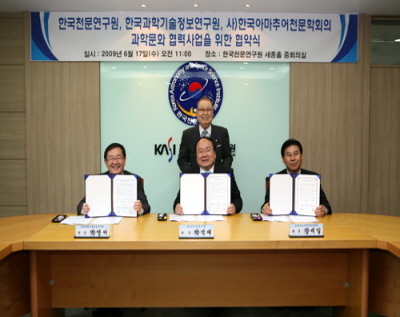
KISTI signs MOU with KASI and KAAS
Korea Institute of Science and Technology Information(KISTI, President Park Young-seo) has concluded a memorandum of understanding on science culture cooperation with Korea Astronomy and Space Science Institute(KASI, President Park Seok-jae) and The Korean Armature Astronomical Society(KAAS, President Jang Se-il). The signing ceremony was held at KASI in Daejeon on June 17, 2009. Under the MoU, KISTI, KASI, and KAAS have agreed to cooperate and collaborate for promotion of SETI Korea(Search for Extraterrestrial Intelligence, Korea), a distributed computing(grid computing) project of KISTI using Internet-connected computers. -
182009. 06
No. 17 View. 5392
Korean Satellite Rocket 'Naro-ho' Close to Lift-off
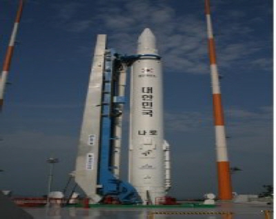
President Lee Myung-bak says "Korea aims to be one of world's top seven space powerhouses in ten years" The nation will see a Korean satellite blast off at a space center built by Korean scientists and engineers as early as late July.At the June 11th inaugural ceremony for the Naro Space Center in Oenaro-do, Yenae-ri, Bongrae-myeon, Goheung-gun, South Jeolla Province, officials from the Ministry of Education, Science and Technology announced, "Korea will launch the 'Naro-ho' (Korea Space Launch Vehicle-1, or KLSV-1), Korea's first satellite rocket, in late July." With the inauguration of the Naro Space Center, Korea became the 13th country in the world to operate a space center. If the Naro-ho is successfully launched, the country will become the world's tenth nation to send a self-developed satellite into orbit. Korea becomes 13th country to operate space center (Photo)The launch pad, standing 33 meters tall, is equipped with a rocket model for performance testing. In his congratulatory remarks at the ceremony, President Lee Myung-bak said, "Korea will continue to invest in research and development for space exploration to usher in a space era on our own in ten years, and become one of the world's top seven space powerhouses." "Fifty years ago, when the U.S., Russia and Europe were advancing into space, Korea was still struggling to overcome poverty and hunger; sending men to the moon seemed to have nothing to do with Koreans," Lee said. "However, Korea has now completed a space center, something operated by only ten countries throughout the world, less than 20 years since we began a space development program, an achievement that we are truly proud of." "Korea will be able to send astronauts into space and to the moon using our own technology in the not-so-distant future," President Lee said, adding, "In order for us to do so, we must speed up the development of a Korean-style rocket launcher based on technology that we have acquired and developed on our own thus far." Urging his fellow citizens to shoot for the stars and embrace a new future for the nation, the president said the successful launch of Naro-ho (KLSV-1), set for late July, would serve as a turning point for Korea to usher in a space era banking on homegrown technology. The ceremony brought together more than 1,000 people, including government officials, lawmakers, senior officials from regional and local governments, and local residents. Korea broke ground on the space center in December 2000, and invested 312.4 billion won over the past eight years to complete the facility. Naro Space Center chief, Min Kyung-joo, said in his progress report, "In the beginning, our researchers relied on Russian technology, but we gradually installed the launch and control facilities using Korea's own technology, and completed performance tests through testing on 14 occasions." Min said the center is conducting launch pad validation testing using a ground validation launch pad, and aims to complete the test by the end of June. According to the Naro-ho launch schedule, the center will also bring in a first-stage rocket model from Russia in June, and complete a second-stage aviation model later in the month. Laser reflector mounted on satellite Lee Joo-jin, President of the Korea Aerospace Research Institute, said, "With the inauguration of the Naro Space Center, Korea has already passed the development phase in the fields of space center design and construction, and entered a utilization phase." Lee added, "Through the successful launch of the Naro-ho, which is scheduled for late July, we expect Korea will demonstrate its capacity in space center operation technology and the capability of its operators in the utilization phase." Lee also said that during the month of July, Korea will complete the assembly of the stage-1 rocket and a second-stage rocket model that will? be actually lifted off, as well as checking off launch preparations, before launching the Naro-ho in late July. Korea's 'science and technology satellite No. 2,' which will be sent into orbit aboard the Naro-ho, will be moved to the Naro Space Center from the KAIST Space Center at 10 a.m. on July 12. Korea's science and technology satellite No. 2 will circle the earth at low altitude orbit (300 km to 1,500 km) for two years. The satellite was developed jointly by the Korea Aerospace Research Institute, KAIST, the Satellite Technology Research Center, and the Gwangju Institute of Science and Technology beginning in October 2002. The satellite, which was developed using homegrown technology, is of small size, weighing about 100 kg. It is equipped with a microwave radio meter that is capable of measuring humidity in the atmosphere and ocean and that was developed by GIST, and a laser reflector that was developed by KAIST and the Satellite Technology Research Center. Lee Kang-bong,editorial board memberaacc409 at naver.com [June 18, 2009]- - - - - - -Source - ScienceTimes -
112009. 06
No. 16 View. 4741
'Artificial Intelligence' to help scientists search science and technology paper...
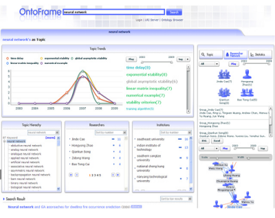
KISTI unveils 'Prototype Next-Generation Science and Technology Information Service' The Korea Institute of Science and Technology Information (President Park Young-seo) said on June 4 that it has constructed a 'Prototype Next-Generation science and Technology Information Service' using OntoFrame, a Semantic service platform and will unveil the system to the public.'Semantic Web' refers to a cutting-edge web service that allows computers to intelligently understand information and then make logical inferences based on different types of data. Onto Frame is a next-generation search platform using Semantic Web technology that allows the user to search the most relevant information through the continual interlinking and seemingly infinite growth of data. The new 'Prototype Next-Generation Science and Technology Information Service' offers in-depth service for 450,000 scientific journals in the fields of information and biotechnology. Specifically, services made available by the innovative system include news on the latest trends in research topics, experts and research institutes by research topic, networks of research sites, and researchers conducting similar studies, information on which is generally hard to retrieve through conventional reference materials and literature. Additionally, the system classifies search words employed by the user according to whether the word is a research topic of a researcher, and allows the user to generate a viewing format suitable for the given search word, thus enabling him of her to locate the required data easily and conveniently. The 'Prototype Next-Generation Science and Technology Information Service' system?utilities more than 40 patents that are being applied for or are already registered in Korea and elsewhere, and has thus earned recognition for its uniqueness and a high level of comprehensiveness. OntoFrame, which was used as the system's service platform, had been applied to projects for the Korea Research Foundation, the Korean Agency for Technology and Standards, and the Ministry of Justice. Ryu Beom-jong, head of KISTI's information technology research division, said, "The new Prototype Next-Generation Science and Technology Information Service will play a crucial role in upgrading the current search-focused information service based on simple keywords to an advanced information service based on Semantic Web technology, a key element for the Web 3.0 era." Meanwhile, KISTI plans to make public the new system via a website(ontoframe.kr/2008) specially designed for the service, and to gather and compile opinions and assay demand for the system to further improve its NDSL service. Photo] Sample web page of the Prototype Next-Generation Science and Technology Information Service (searched through "neural network") ? Hellodd.comJung Ji-onjion97 at hellodd.com [June 11, 2009]--------------Source - Hellodd.com -
272009. 05
No. 15 View. 6107
ETRI develops core technology for 'high-efficiency white OLED lighting'
New technology boasts electricity consumption efficiency of over 70 1m/W. Expected to carve out global lighting market niche worth 3 trillion won.(Photo) ETRI-developed OLED lighting, considered on par with Korea's best OLED lighting technology. A Korean research team has developed a core technology for Organic Light Emitting Diode (OLED) lighting, an eco-friendly 'green growth' lighting technology that is replacing conventional florescent lamps and glow lamps.The Electronic and Telecommunications Research Institute (ETRI, President Choi Moon-ki) said on May 20 that it had developed a white OLED lamp for lighting that boasts an electricity consumption efficiency of 70 1m/W, the highest level in Korea. OLED technology is considered an exemplar of "eco-friendly green growth" lighting due to its energy efficiency, which is higher than either florescent lamps or glow lamps, reduced carbon dioxide emission, and non-production of mercury, a by-product of both florescent and glow lamps. Numerous countries around the world are currently racing to develop OLED lighting together with other next-generation lighting devices, including LED lighting. OLED lighting is not only thin and lightweight, but it also offers a transparent and flexible lighting source. Hence, it is a highly versatile technology. with numerous potential applications owing to a host of advantages in terms of its high efficiency, long durability, low cost and lighting design. ETRI said the development is notable in that Korea has now secured a high level of technology in the white OLED lighting sector that is on par with that of advanced countries. Korea had previously been saddled with a more than five-year technology gap in the sector in relation to those countries. Experts say that the development will also allow Korea to join the race for high-performance lighting, which has traditionally been led by advanced countries, and to advance the commercialization of OLED lighting by banking on the new technology. Cho Hye-yong, head of the ETRI's OLED lighting research team, said, "OLED lighting shares the same industry infrastructure and value chain as the OLED display, and if Korea can proactively take advantage of its industrial environment as the top producer of OLED displays, it will be able to dominate the next-generation lighting market." In the meantime, ETRI plans to hold an "OLED lighting design contest" from May 25 to August 31 in an effort to promote and propagate OLED lighting. ETRI will seek to hold the contest as an annual event, and identify talented designers and excellent designs that make the most of OLED technology as a flat lighting source. The Institute expects excellent designs and talented designers will contribute to the early industrialization of OLED lighting by making the most of Korea's superior OLED production infrastructure. The institute plans to make prototype products based on the contest's winning designs, and exhibit them at the "IMID international display exhibition" in October in order to promote OLED lighting. (Photo) Poster for the OLED lighting design contest. ? Hello DD.comLim Eun-heeredant645 at hellodd.com ? [May 27, 2009]- - - - - - -Source - HelloDD.com