 Delete Article!
-
042011. 10
No. 58 View. 16450
Scientist Resolve Decade-long Puzzle of 'Protein Function'
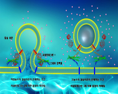
Scientist Resolve Decade-long Puzzle of 'Protein Function' The Ministry of Education, Science and Technology(Ahn Byung-man, Minister) said on May 7 that a research team led mostly by Korean researchers had identified for the first time that Synaptotagmin1, a plasma membrane protein, proactively regulates the communication processes of nerve cells. Study published in world's top journal, Science Synaptotagmin1 is one of two major proteins that regulate the excretion of neurotransmitters. Thus far, the research community has speculated that simple introduction of calcium ions leads Synaptotagmin1 to excrete neurotransmitters, but has failed to identify its exact functions. In the study led by Prof. Yoon Tae-young of KAIST, the researchers identified that Synaptotagmin1 serves as a switch that freely regulates the intensity of communication between nerve cells. The research team confirmed for the first time that the introduction of calcium ions at an appropriate density level(10umol/L) into nerve cells causes Synaptotagmin1 to swiftly excrete neurotransmitters, but that contrary to expectations, their introduction at above the appropriate density level decreases the function. This indicates that Synaptotagmin1 responds in various fashions according to the density of calcium emitted from nerve cells. Thus, the scientists have newly discovered that Synaptotagmin1 can freely control the intensity of communication between nerve cells. The new study has discovered for the first time that Synaptotagmin1 most robustly activates at a low calcium density level, and precisely explained the function of Synaptotagmin1, a puzzle that previous studies had failed to resolve. The research team also identified that the detachment of Synaptotagmin1 from membranes leads to the loss of its regulatory switching function, thus discovering that the attachment and non-attachment of Synaptotagmin1 onto and from membrane comprise the centerpiece of its function. Furthermore, Prof. Yoon's research team successfully developed a new technology that allows scientists to monitor the functions of membrane proteins, which are a major target in the quest to develop next-generation new drugs. According to the ministry, membrane proteins play essential roles within the cell, including substance transport, and are closely related with diverse diseases, including cancer, diabetes, and obesity. Hence, they account for up to nearly 70% of the target proteins in the effort to develop new next-generation drugs. The team successfully developed single-vesicle fluorescence detection, and thus secured internationally top-flight technology that allows them to monitor the function of membrane proteins at single-molecule or multi-molecule levels. Prof. Yoon said, "The study has identified the function of Synaptotagmin1, which the academic community has failed to decipher over the past 10 years, and has developed a new technology that enables us to monitor the complicated functions of membrane proteins at the molecular level." Expounding on the significance of his research, he added, "The study has tapped the possibility to develop new drugs for diseases afflicting people of the modern world, including cancer, diabetes and obesity." The study was conducted jointly by nine researchers, including Prof. Yoon, Dr. Lee Han-ki of POSTECH, Prof. Shin Yeon-kyun of Iowa State University, Prof. Kweon Dae-hyuk of Sungkyunkwan University, and Prof. Hyeon Chang-bong of the Korea Institute of Advanced Study. The study was published in the May 7 issue of Science, one of the world's top science journals. [May 31, 2010] - - - - - - -Source - HelloDD.com -
042011. 10
No. 57 View. 17595
New Fundamental Technology Increases Light Extraction Efficiency by 30%
New Fundamental Technology Increases Light Extraction Efficiency by 30% A Korean research team has opened up the possibility to preoccupy the global LED lighting market. The Ministry of Education, Science and Technology(Ahn Byung-man, Minister) said a Korean research team had developed a fundamental technology that increases the light extraction efficiency of InGaN green LED, a next-generation lighting source, by more than 30%. Korean researchers increase green LED's efficiency to carve out global lighting market Indium Gallium Nitride (InGaN)Materials essential for forming active layers for white, blue, green, ultraviolet-ray LED The study, which was led by Prof. Jung Gun-young from the department of new materials engineering at the Gwangju Institute of Science and Technology, and senior researcher Jeong Mun-seok of GIST's Advanced Photonics Research Institute. The study was conducted with support from the Basic Science Research Program and the Nano R&D Program, which are operated by the Ministry of Education, Science and Technology and the Korea Research Foundation. The study was published as 'frontispiece' in the April 9 issue of Advanced Functional Materials. LED, a next-generation lighting source, is a green energy technology that is highly sought after because of its high energy efficiency and eco-friendliness. Unlike conventional lighting such as light bulbs and florescent lights, LED technology presents high efficiency in the conversion of electric energy into light energy, and thus helps cut energy consumption by up to 90%. If Korea replaces 30% of its lighting needs with LED lighting, the country can cut 16 billion kWh(volume equivalent to power generation volume of two 1 million kW-class nuclear power plants) from its electricity consumption, and effectively reduce 6.8 million tons of carbon dioxide emission. "Aiming to preoccupy US$110 billion market by integrating with subsequent research" The newly developed technology does not degrade the electrical characteristic of LED, when compared with the conventional LED, but rather increases light emitting efficiency by more than 30% through the "photo wave guide" effect in zinc oxide(ZnO) nanorods. The photo wave guide effect refers to a technology that increases LED efficiency by creating a photo wave guide, a route through which light travels, in the LED device. The researchers cultivated ZnO sub-microrods using a hydrothermal method on an ITO top contact layer of InGaN green LED(light emitting diode). Subsequently, the researchers investigated whether ZnO nanorods efficiently absorb and emit light generated from the LED by using a micro microscope they developed on their own. Hydrothermal methodA method of synthesis conducted by melting a reactant in water and heating it up at temperatures below 100 degrees Celsius As a result, the researchers discovered that when LED emits light, light transmitted via ZnO nanorods was efficiently extracted at the tip of the rods. Through this experiment, the research team demonstrated that ZnO nanorods served as a route for light transmission, and thus increased the light emitting efficiency of the LED structure. Prof. Jung Gun-young said, "With the study, we have developed a fundamental technology that drastically increases light emitting efficiency in the aspect of materials costs and processing costs," adding, "If we fuse this technology with the results of our subsequent studies, we expect that Korea will be able to preoccupy the global LED lighting market, which is projected to reach US$ 110 billion in 2015." ? Kim Chung-hanchkim at kofac.or.kr [May 10, 2010] - - - - - - -Source - ScienceTimes -
042011. 10
No. 56 View. 21425
'Hepatitis B Treatment' with Indigenous Natural Plant Developed
Liver disease is the biggest cause of death among people in their 40s and the third-biggest cause among those in their 30s. Hepatitis B infection is a major cause of chronic liver disease, with the virus isolated in 73 percent of patients with chronic hepatitis and cirrhosis, and 77 percent of patients with primary liver cancer. KRIBB Dr. Lee Young-ik seeks 'zero' mutation by utilizing indigenous natural plant. Likewise, patients infected with hepatitis B, if left untreated, are effectively constantly exposed to the risk of developing liver cancer, which is caused by the virus. Many anti viral drugs, including lamivudin and interferon, which are commonly used to treat hepatitis B, are widely available in the market. Interferon temporarily increases immunity, while Lamivdin suppresses the activity of DNA polymerase, and curbs its reproduction, resulting in temporary efficacy of treatment. However, when used for a long period of time, this drug allows for the mutation of hepatitis B virus, rendering it resistant to the treatment, while e-antibody continues to be excreted. As a result, a high portion of hepatitis infection progresses into Liver cirrhosis and liver cancer. For this reason, doctors have had to take the trouble of prescribing alternative treatments to patients, coincidently with the emergence of the mutated virus. Dr. Lee Young-ik at the Korea Institute of Bioscience and Biotechnology(Park Young-hoon, President) developed a treatment that suppresses the cause that triggers different mutations to address the problem. At the start of his research, Dr. Lee set the goal of developing a drug for suppressing the emergence of the mutated virus at the time of the secretion of e-antibodies, the integration of hepatitis B virus and liver cancer, and the reproduction of Polymerase, while retaining the efficacy of conventional treatment. In order to develop a new drug, Lee's team first searched for a material that has a suppressing effect. His effort to develop hepatitis B treatment saw no gain through genetic methods or chemical approaches that he had researched previously. Subsequently, learning by change that certain indigenous plants have efficacy, he began research using such plants in earnest with support from the New Frontier R&D Program Plant Diversity Research Center(Joung Hyouk, Director) from 2006. Dr. Lee singled out 135 plant species, which had been used in treating liver disease since ancient times, from the plant extract bank of the New Frontier R&D Program Plant Diversity Research Center. Of these, he singled out eight plant species that were found to directly remove the hepatitis virus, and finally selected on three indigenous plants, including Phyllanthus Urinaria Koreana. He then extracted virus-suppressing substances from the indigenous plants, developed a treatment and conducted animal tests. The substance effectively lowered the portion of mutations, which stood at as high as 10^6/1 to 10^18/1, which is far superior to conventional treatment. "The most important thing in the development of the treatment is the fact that we have developed substances that suppress mutations at different points in time from the three indigenous plants. Based on these substances, we have developed treatments whose operational mechanisms are completely different from those of conventional anti-viral drugs." His study is currently undergoing tests for safety and efficacy. In particular, noting that the hepatic B virus in pregnant women can be transmitted to the fetus, he injected the new treatment into cubs given birth by animals with the virus, and is conducting experiments to determine how the treatment affects the cubs with the virus. Dr. Lee said, "Considering the results of efficacy tests and the development process thus far, we anticipate positive findings from the safety evaluation process," adding, "When we finish animal tests, we will begin a process for the treatment's commercialization in earnest in accordance with the rules and regulation of the Korea Food and Drug Administration." Dr. Lee, who has researched viruses for more than 20 years, aims to develop treatments for Cirrhosis and liver cancer, on top of treatments for hepatitis B. "Since the liver is a central organ of humans, I would like to concurrently study metabolic diseases as well. Just as we were able to generate promising research with support from the New Frontier R&D Program Plant Diversity Research Center, I hope that well-organized research support programs with similar purposes can provide ample assistance to researchers." Kim Hee-jin [April 26, 2010] - - - - - - -Source - HelloDD.com -
042011. 10
No. 55 View. 16845
New Process for Synthesizing Metal Nanoparticles Developed
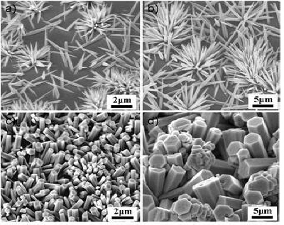
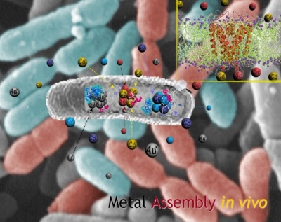
Korean researchers have developed a new process that allows for synthesis of metal nanoparticles of diverse sizes and kinds through a novel bioengineering method. 'New technology to allow for creation of metal nanoparticles using microorganisms' Prof. Lee Sang-yup and research professor Kim Tae-jung of KAIST(Suh Nam-pyo, President) said on September 1 that they had developed a technology that allows for the production of quantum dots and magnetic nanoparticles, and metal nanoparticles of diverse types, which had previously not been synthesized, by regulating the secretion of heavy metal-absorbing protein in E-coli and peptides; the technology also allows for free control of the size of metal nanoparticles by adjusting the density of metallic ions that are added in the process. The study was published on August 18 in the online edition of Angewandte Chemie International Edition, a world-renowned chemistry journal, and was introduced as a "hot paper," earning recognition for its significance. Prof. Lee Sang-yup and research professor Kim Tae-jung The researchers excreted metallothionein, a protein that binds with metallic ions, and phytochelatin, a peptide, either independently or through combinations in E-coli, and exposed diverse metallic ions to the cultured fluid, thus generating diverse metal nanoparticles. By regulating the excretion of metal-binding protein, and the density of metallic ions, the researchers generated quantum dot, nano-magnet, and gold nanoparticles of diverse sizes, as well as metal particles that had never before been chemically synthesized. If recombinant E-coli cells are separated through centrifugation and crushed, thus removing various organic substances, only the synthesized metal nanoparticles can be acquired easily. By attaching diverse bioactive materials to the surface of these metal nanoparticles, the researchers presented the possibility of using biologically synthesized nanoparticles for research on various drug delivery systems and developing medical diagnostic tools that use animal cells. Prof. Lee said, "The study presented a technology that allows for efficient and convenient synthesis of desirable nanoparticles through biotechnological culturing of recombinant microorganisms instead of the conventional physical and chemical process," adding, "The technology will have diverse applications in medicine and bioengineering research in the future." The study was conducted with support from the World Class University program, which is operated by the Ministry of Education, Science and Technology(Lee Ju-ho, Minister) and the Korea Research Foundation(Park Chan-mo, Chairman), and from the "Industrial Fusion Technology, Industrial Core Technology Development Program" sponsored by the Ministry of Knowledge Economy(Choi Kyung-hwan, Minister). Kim Josephjoesmy at HelloDD.com twitter: at ssebiU [September 27, 2010] - - - - - - -Source - HelloDD.com -
042011. 10
No. 54 View. 17559
Carbon Nanotube Thread Korean Researchers Developed
Korean researchers have developed a production technology for 'carbon nanotube thread,' a high-tech material. The Ministry of Education, Science and Technology(Minister Lee Ju-ho) said on February 16 that a research team led by Prof. Nam Seung-hoon of the Center for Nanoscale Mechatronics and Manufacturing under the 21st Century Frontier Research and Development Project had succeeded in developing carbon nanotube thread. The study was published as the cover paper in the January 1, 2011 issue of Carbon, an international science journal. Seek to industrialize new material into functional composite materials, including those for bulletproof vests, aerospace components Carbon nanotube thread, which is less than 1 micrometer(one 100th of a hair strand) thick, is comprised as bundles of multiple strands of successively integrated carbon nanotube. Carbon nanotube thread is a material which is less than 1 micrometer thick. Since it boasts high elasticity and strength(some 100 times that of steel), it can be applied in diverse fields. Dr. Nam's research team cultivated carbon nanotube vertically on a silicon board, formed bundles of multiple strands of carbon nanotube from it, and then reeled the substance into the form of thread to create carbon nanotube thread. By applying voltage, the research team also succeeded in photographing the real-time change in shape that occurs on the tip of the carbon nanotube thread when electrons are emitted. The technology allows for the reeling of multiple strands of carbon nanotube thread at once, or the easy coating of polymer substances on carbon nanotube thread. It also allows the material to be produced in sheet type as well as in thread form, thus making it possible to produce carbon nanotube film. Carbon nanotube is flexible and highly conductive, and can thus be used as a material for touch screens. By taking advantage of its characteristic of emitting heat on the surface when a current is applied, the material can also be used in heaters to prevent fogging on automobile glass. Kim Chung-hanchkim at kofac.or.kr [February 23, 2011] - - - - - - -Source - ScienceTimes -
202011. 09
No. 53 View. 17533
New High-precision Distance-measuring Technology Capable of Measuring 1nm Gap at...
New High-precision Distance-measuring Technology Capable of Measuring 1nm Gap at Range of Hundreds of km. A Korean research team is drawing keen attention by developing a high-precision distance-measuring technology that is capable of measuring a gap of 1nm at a distance of hundreds of km. KAIST develops core space technology, 'opens possibility for Korea's leap toward becoming nation of advanced space technology' The research team led by Prof. Kim Seung-woo from KAIST's Department of Mechanical and Aerospace Systems said on August 17 that it had developed a revolutionary high-precision distance-measuring technology that is capable of measuring in the 1nm range, overcoming the conventional resolution limit of 1mm in measuring long distances. 'Resolution limit' refers to the smallest unit of physical volume that a gauging device can possibly measure. A resolution limit of 1mm refers to a unit at which a device can measure the gap of 1 mm from a distance of several hundred km. The technology developed by Prof. Kim's team also overcomes the ambiguity that generally appears when measuring over long distances, and thus the technology theoretically can measure a distance of 1 million km without ambiguity. In fact, the team successfully attained a 150nm resolution limit at a distance of 700m, and demonstrated that the new technology can allow for a resolution limit of 1nm in a vacuum state such as that which exists in space. The study will bring scientists a step closer to the operation of a satellite fleet(the launch of small multiple satellites to measure the distance between satellites, and eventually to find a planet similar to the earth, or to verify the theory of relativity) aimed at discovering a planet similar to the earth; it also advances the possible development of future space technology for measuring distances between planets, and for verifying the theory of relativity. High-precision measurement of distances between satellites and planets is a core technology in humanity's quest to find a planet similar to the earth or to verify the theory of relativity, and countries with advanced space know-how are scrambling to develop and secure such technology. In explaining the significance of his study, Prof. Kim said, "With the development of technology that is capable of measuring distance at a resolution limit of 1nm, Korea has secured high-precision distance-measuring technology, a core part of future space technology such as that involving the operation of a satellite fleet," adding, "Korea has thus laid the foundation toward joining the league of countries with advanced technology." The study was published on August 8 in the early online edition of Nature Photonics, a preeminent scientific journal in photonics. Lim Eun-heeredant645 at HelloDD.com twitter: at redant645 [September 03, 2010] - - - - - - -Source - HelloDD.com -
262011. 07
No. 52 View. 16663 Since 1962, KISTI has played a role of National Science & Technology Information Center to provide information that researchers need to enhance the national competitiveness as a specialized science & technology research institute supported by the government. On the occasion of its 50th anniversary, KISTI as a science & technology information institute, will lead the way in making Korea a powerful science & technology country.

-
212011. 07
No. 51 View. 16144 For those of you with hearing difficulty please read the video script below. When human being was blind to science and technology,we had to travel far to acquire knowledge.Today, we are sharing scientific knowledge handed down for generations with the rest of the world. Those who were there to witness the beginning of Korea’s miracleThose who now prepare for the next 50 years with inheritance of 50 years The Korea Institute of Science and Technology Information - KISTI!Here is our story. In 1960s when Korea was a poor nation with GNI per capita of less than 100 dollars, it seemed like poverty and hunger would last forever.Science and technology was the key to overcoming poverty and reviving Korea. In January 1962, Korea’s first Science & Technology Information Center was established to develop Korea’s science technologies and economy. In a country that was a wasteland for science and technology and industrial infrastructure, KISTI became a trailblazer, experiencing both the joys and hardships of Korean companies during the journey to achieving Korea’s unbelievable economic miracle. Leading Korea from a nation of poverty to one of the top 10 economic powerhouses in the world, KISTI has laid strong foundation in Korean science and technology.This is what makes KISTI’s 50-year history so special,and why we eagerly look forward to the next 50 years.there were those who shared every moments in Korean history. Over the past 50 years, KISTI has led the way in building Korea’s national science, technology and knowledge information infrastructure. By collecting and providing advanced science & technology information and producing value-added information through industrial and technology information analysis and establishing a next-generation research environment based on high-performance supercomputers, KISTI is playing a crucial role in making Korea one of the science and technology strong countries of the world. Science & Technology Information DisseminationIn an environment where information is created every year,KISTI is striving to provide optimized, high-quality science & technology information. Through Korea’s largest science and technology information portal NDSL,KISTI has established a database of over 100 million science and technology information-related contents and is providing up-to-date information by utilizing semantics-based searching technology.? And by establishing KESLI, which is a national level electronic information joint purchase consortium, KISTI has purchased 26,000 electronic journals with 550 organizations including universities and companies, resulting in reduction of approximately 1 trillion won in expenses. Furthermore, the National Technology Information Service (NTIS) which is designed for shared use of national R&D information is preventing overlapping R&D investments and maximizing R&D investment efficiency and productivity. Information AnalysisKISTI is also providing value-added information analysis services to cope with demands in a timely manner in today’s rapidly changing information environment and to support corporations in establishing optimum strategies and focus on technology developments. By establishing various support programs for supporting customer success through technology commercialization, KISTI is discovering prominent technologies that will lead Korea’s future and is sharing technology commercialization know-how. The Promising Future Technology Seminar, which is hosted by KISTI ever year, is evaluated as Korea’s leading science and technology information seminar for companies to see the latest technical trends and to establish future strategies in today’s era of intense global competition. By providing new business opportunities to SMEs and competitive information analysis models, KISTI is becoming a stepping stone for SMEs to become global enterprises. SupercomputingBy introducing and operating the 360 teraflops Supercomputer, KISTI, as a national supercomputing center, is serving a core role in strengthening Korea's S&T competitiveness. By establishing the state-of-the-art national R&D network KREONET, KISTI is connecting 16 key regions of Korea and 28,000 research institutes in the world. This state-of-the-art cyber research infrastructure allows research institutes to share research resources without restrictions of time or space. By utilizing this cyber infrastructure to provide an environment in which Korean researchers can utilize data created from the world’s three largest accelerators and enormous CPU resources access, KISTI has created a research environment for Korean researchers to easily begin large science research projects on a global scale. By developing the high-tech science education hub, Edison System, KISTI is allowing engineering major students and industry personnel to simulate their latest research achievements online, which allows highly-qualified engineering manpower to begin research early and to save time and re-education costs. SME SupportKISTI's mission is also to make Korean SMEs into strong enterprises. By establishing the Association of Science and Technology Information (ASTI), which is a nationwide industrial-academic-research collaboration network , KISTI is providing information support as well as technology and product development support using KISTI’s supercomputer. By visiting 100 SMEs on site and designating one KISTI researcher for each SME to provide R&D support, KISTI has dramatically reduced the R&D period for SMEs that experience manpower and information shortages. And by utilizing supercomputers in SME technology and product development, KISTI has cut down the time and cost for manufacturing a product, which ultimately supports SMEs to become strong enterprises. ? ? To achieve the vision and goal of becoming an “Global S&T Information Research Institute that creates customer values”, KISTI is promoting its new 4S core management values. As the root of Korea’s science and technology, KISTI has contributed to Korea’s scientific development by creating greater customer values. Having served at the center of science and technology information over the past 50 years, KISTI is preparing to soar to greater heights in the next 50 years. KISTI is made by people.And KISTI is made for the people.? The new future of Korea!The next 50 years of science and technology!KISTI will lead the way!
-
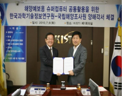
062010. 07
No. 50 View. 14803 Supercomputer will be used in developing forecasting model for massive marine disaster and climate changes. Korea Hydrographic and Oceanographic Administration (KHOA) and KISTI agreed to cooperate in utilizing national supercomputing resources and science and technology information. KHOA is in charge of national marine information and its service and it will use KISTI supercomputer to develop high-resolution marine forecasting model necessary for precise marine weather forecasting.
-
182010. 06
No. 49 View. 15440
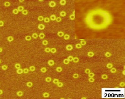
POSTECH develops nano-size 'doughnut' structure assembly
Technology to allow for synthesis of nano-size metal; chosen as notable study by Nature journal World-renowned chemistry journal 'Angewandte Chemie' carries study on front cover (Photo)Doughnut-shaped nanostructure assembly. Korean scientists have developed a new polymer nanostructure in the shape of a doughnut that is consistent in size, and is different from nano-metal particles of different shapes, including globular, cylindrical, disk and spiral shapes. Pohang University of Science and Technology (President Baek Sung-gi) said on June 11 that its research team led by Profs. Chang Tai-yun and Huang Hai-ying at the Brain Korea 21 molecular science initiative had developed a technology that allows for the production of nano-metal particles by employing as nanotemplate doughnut-shaped molecular assemblies that are consistent in size through the use of spontaneous self-assembly of diblock copolymers. Chang's team succeeded in creating a pure, consistently sized, doughnut-shaped nanostructure assembly (ring-closure products of rod-shaped micelles) based on a nanostructure assembly that was poor in utility due to the uncontrollability of its structure and size? by applying diblock copolymers with a low glass transition temperature, and a selectively reacting solvent mixture. The new structure assembly is drawing keen attention because it not only maintains the structure in the solvent mixture for several months, but also allows the nano-metal particles, which were created through careful manipulation of their size and shape, to be inserted into a specific location of the nanostructure assembly. If researchers synthesize nano-metal particles, which can be created to be consistent in size and shape, they can generate a new nano-compound of sophisticated shapes much more easily than via conventional methods.Moreover, since it allows researchers to easily generate a nanostructure assembly that is consistent in size, the technology is expected to make major contributions to applied research in related fields, including the development of next-generation nano-scale memory devices. The study was selected as the "VIP" and cover thesis in the latest issue of Angewandte Chemie, the world's preeminent chemistry journal published by the German Society of Chemistry (the Gesellschaft Deutscher Chemiker). The study was also introduced as a 'notable study' in the polymer chemistry field in the 459th issue of the journal, Nature, reflecting the keen attention the technology has attracted from international academia. (Photo)From left: Prof. Chang Tai-hyun, Prof. Huang Hai-ying (lead author), Ph.D. candidate Jung Ju-eun, Dr. Park Hae-woong. ? Lim Eun-heeredant645 at hellodd.com[June 18, 2009] - - - - - - -Source - HelloDD.com