 Delete Article!
-
182012. 01
No. 64 View. 24139
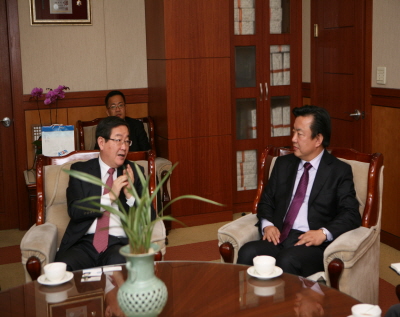
President of ACTS visited KISTI
KISTI has welcomed Mr.Lee Hyo-jeong, President of ACTS(Daejeon Agency of Advanced Cutural Technologies and Service) and his visiting group on Jan.10th at its head office located in Daejeon. ACTS was built as the agency of Daejeon city in 2007 to promote medial industry and cultural events in Daejeon city. Mr.Lee,President of ACTS was given a brief introduction of KISTI R&D activities and had a field trip to KISTI supercomputing center. After that, Dr. Dr.Park Young-seo, President of KISTI and Mr.Lee had a discussion on mutual cooperation for supporitng media industry with KISTI supercomputer. -
062012. 01
No. 63 View. 24080
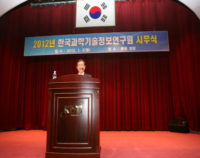
KISTI Kick-off meeting for 2012
KISTI hold a kick-off meeting for 2012 at its head office located in Daejeon. At the meeting, Dr.Park Young-seo,President of KISTI emphasized the importance of year 2012 as KISTI will celebrate its 50th anniversary of its foundation on May 18th. At the speech, Dr.Park appreciated KISTI staffs for their efforts and contribution to the remarkable and excellent R&D performance made in 2011. After the meeting, Dr.Park and executive managers shook hands with every staff participating the meeting wishing the best luck for year 2012. -
042011. 10
No. 62 View. 30685
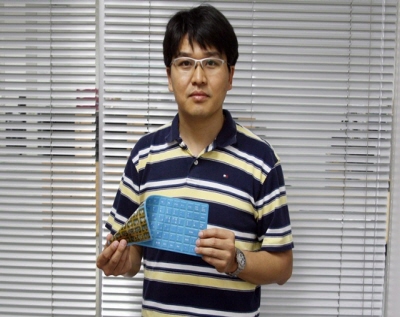
'Having Fun, Relaxing,' Researchers Create Profitable Keyboard
'Having Fun, Relaxing,' Researchers Create Profitable Keyboard The development of a 'power-free, wireless keyboard' was not an official research project of our institute. It was created by chance. "We did not start our project with the intent of developing a power-free, wireless keyboard. In reality, the product's creation simply happened in the course of our enjoying our R&D work. We're excited that we came to transfer the technology in order to come a step closer to its commercialization." Chung Sung-kwan, chief of future device team, KAIST Institute for IT Convergence, develops 'power-free, wireless keyboard technology' 'Ideas' discussed in taskforce meeting lead to 'exciting development' So says Chung Sung-kwan, head of the future device team at the KAIST Institute for Information Technology Convergence(chief Cho Dong-ho), which operates under the KAIST Institute(Director Kim Sang-soo). Chung developed a "power-free, wireless keyboard," which can operate without a power supply and a cord, and successfully transferred the technology to a company, drawing attention from people within and outside the research community. The keyboard is a device that operates wirelessly, even without a built-in power source. Unlike wireless keyboards that are on the market, this device does not require a battery. In order for us to use a computer, diverse peripheral devices are required, including output units such as a monitor and printer, and input devices, such as a keyboard and mouse. Such supplementary devices also include a portable hard disk and USB memory, which are used to increase the user's convenience in data storage. However, all these devices require a cable to supply power. Without a cable, power cannot be supplied and data cannot be stored or moved. So what is the mechanism of the "power-free, wireless keyboard" that has been developed by Chung and his team?The secret lies in RFID(Radio-Frequency IDentification) technology. Using mobile RFID tag technology, the new device allows the computer to recognize the pressing of keys. RFID refers to a technology that allows for remote recognition of data by using electro waves, a process that requires an antenna for data transmission and reception. RFID is commonly used in our daily living. RFID chips are contained in bus and subway public transportation cards, and in the security key buttons in new clothes that prevent shoplifting. Common keyboards contain some 80 to 110 keys. These keys are linked to circuits at the bottom, and whenever keys are pressed, the signs are displayed on the monitor, which is an output device. Both desktop computers and laptops operate through this mechanism. The keys on the power-free, wireless keyboard are the same as those on normal keyboards in the way they are linked to circuits. However, the new keyboard's individual keys, each measuring 2cm, each contain a built-in antenna that transmits data to the keyboard, and a RFID chip. The chip is about 2 mm long and 2mm wide. When a user inputs data through keys on a power-free, wireless keyboard, the keyboard receives the data via a Reader. Upon receiving this data, the Reader sends the signals to the software. At the same time, it constantly scans the data(reading) at speeds of up 10 to 20m/sec. Another characteristic of the power-free, wireless keyboard is "flexibility." Since it uses a film-type polyimide and can be produced in the form of printed circuit boards, it can be rolled and folded, a feature that makes the device easy to carry. Also, since individual keys operate independently, it is possible to use the keyboard even when it is folded, bended, or randomly compressed. Chung Sung-kwan, chief of the KAIST Institute for IT Convergence, who developed the 'power-free, wireless keyboard' Individual rectangles constitute the keys. The dark part functions as an antenna, while the smaller chip on the right is an RFID chip The development was made possible thanks in large part to the support of KAIST professors Cho Dong-ho of the department of electrical and electronic engineering(Director of IT fusion research center) and Yoon Chun-sup from the department of physics. Prof. Cho first suggested the idea of a wireless keyboard and incorporated key recognition technology adopting the RFID method to add to momentum to the device's development. Prof. Yoon examined the structure and physical characteristics of the material used in the keyboard to ensure that data could be communicated even if the keyboard were bended or folded. # 'Ideas on wireless keyboard popped up while chatting' The idea for a power-free, wireless keyboard started with a "story." It is the result of rather uncanny imaginations. The KAIST Institute for IT Convergence runs a "future terminal taskforce," which is comprised of the future device team and professors in related fields. The taskforce was created with a view to examining "things that will have a major impact on the market," and "items that can spearhead technological advance and that users need." The idea popped up when taskforce members were chatting about submissions to a "Contest on future terminal ideas," which the IT Convergence Institute conducted for its researchers in 2007. While running the taskforce, team leader Chung Sung-kwan was carrying out a project entitled "User interface technology concerning future IT device transformation." The objective of the project had nothing to do with the development of the power-free, wireless keyboard. The keyboard was developed while the taskforce was conducting this research project. Whenever they faced obstacles in conducting the project, taskforce members gathered to discuss how to sort things out. A smiling Chung said, "While conducting research projects, we often face situations where we can't effectively address challenges and get headaches." He added, "Whenever we had such problems, we diverted our efforts to focus on the development of the power-free, wireless keyboard to relax and ease our headache and to draw the public's attention." In short, the keyboard was effectively a "fun development," which taskforce members returned to for relaxation whenever they felt bored or developed a headache about their research projects. Chung Sung-kwan conducts a demonstration on his own. Whenever the small keys were pushed, letters were presented on the display. # Transferring technology to a company, developers 'seek to focus on the acquisition of core technology, instead of minimal technology transfer fees' The KAIST institute for IT Convergence transferred the "power-free wireless keyboard technology" via P&IB's Daejeon branch(Kang In-gyu, branch chief) to Hanyang Semitech in Gyeonggi Province on July 18. The contract entailed 30million won in technology transfer fees and 3% of running royalty fees. Chung said, "We developed the keyboard to acquire a core technology at the school, not to transfer technology, and had no intent for technology transfer in the first place." He added, "Rather than focusing on the fact that we transferred the technology, we will seek to address the technology that the company needs and the problems it must resolve when commercializing the transferred technology." Chung plans to continue supporting Hanyang Semitech over the next two years to help commercialize the technology. You Sang-youngyoung at HelloDD.com twitter: at SangYoung25 [August 12, 2010] - - - - - - -Source - HelloDD.com -
042011. 10
No. 61 View. 29966
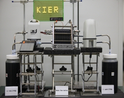
5kW-class 'Redox Flow Battery' Developed
5kW-class 'Redox Flow Battery' Developed Amid growing worldwide attention to large-capacity secondary battery technologies, a Korean research team has developed and successfully demonstrated 5kW-class Redox Flow Battery technology. Core technology developed for production of large-capacity rechargeable batteries A Redox Flow Battery(RFB) is a rechargeable battery that can store energy for an extended period of time by repeating recharge and discharge processes. Theoretically, there is no limit to its lifespan, with longevity known to be more than 10 times that of a lithium-ion battery. The developed device is a new-concept, next-generation battery that can increase the duration of power usage as much as desired according to the battery's capacity. The Korea Institute of Energy Research(Han Moon-hee, President) said on July 15 that it had developed and successfully tested for the first time in Korea 'RFB technology,' which is emerging as the most promising system among large-capacity rechargeable batteries. According to the institute, a demonstrative test found that the battery exhibits a level of output performance on par with that of world-class products, with its efficiency shown to be 5 to 10% higher. The newly developed RFB system is comprised of a stack and an electrolyte tank. The stack, where chemical reactions occur, can be operated at normal temperatures, and thus can be used for over 20 years. It adopts vanadium as its active substance and can be used semi-permanently, thus meeting the conditions of a rechargeable battery in terms of safety, lifespan, and disposal. The development of the new system is significant in that it allows for stable electric power supply(stabilization of output) by addressing problems with the generation system of renewable energy, which could not supply energy in a continuously stable fashion due to being affected by significant output fluctuations tied to the surrounding environment and natural conditions. The RFB system is highly sought after as a promising next-generation energy-storage technology due to the huge potential for its advancement: it can be applied to renewable energy power generation systems, power plants, blackout-free power supply systems in buildings and semiconductor plants, and a power source for unmanned communication sub-stations. When its energy density is increased, it can also be used in electric vehicles. The institute has developed recharging systems for electric vehicles for over 10 years, and has been conducting research and development activities in the large-capacity battery field, encompassing the development of core technology for large-capacity RFB, cultivation of human resources, and consultation for industries. Dr. Jin Chang-soo, principal investigator at the Energy Conversion and Storage Research Center, said, "The achievement is expected to serve as a catalyst for the transition of research in Korea on large capacity rechargeable batteries into the phase of full-fledged technology development." Jin added, "Going forward, the institute will aggressively conduct follow-up studies aimed at optimizing processes and securing enhanced long-term performance in order to assure the durability and economic viability of the battery, which are required for its actual industrialization." ? Kim Joe-sephjoesmy at HelloDD.com twitter: at ssebiU [August 02, 2010] - - - - - - -Source - HelloDD.com -
042011. 10
No. 60 View. 27200
Chollian Satellite to Operate through Purely Homegrown Control System
Chollian Satellite to Operate through Purely Homegrown Control System Korean scientists have developed a control system that can remotely monitor and operate the Chollian, Korea's first geostationary satellite, using purely homegrown technology. The Electronics and Telecommunications Research Institute(Kim Heung-nam, President) said on June 29 that the Chollian, which was successfully launched on the morning of June 27, will be operated via a control system that was developed by the institute. Korean breakthrough secures technological independence in geostationary satellite control systemTechnology on par with advanced technology overseas, seen as potential export With the successful development of a control system for the Chollian, Korea has thus become a space technology powerhouse with the capacity to develop a control system for geostationary satellites, following the development of a control system for low earth orbit(LEO) satellites such as the Arirang. Under a specific project for a communication, oceanic and meteorological satellite communication system, which was coordinated by the Korea Communications Commission, Korea has successfully made the astonishing achievement of developing not only a satellite control system, but also a communications transmitter and a satellite earth station through homegrown technologies. 13-meter TTC antenna and control communication equipment - TTC sub system The new satellite control system comprises?# a 'TTC TTC, or Tracking, Telemetry, and Command sub-system', which includes a 13-meter antenna for the remote measurement, including that of distance, and remote command necessary for communication with satellites,?# a 'real time operation sub-system' designed to monitor in real time the conditions of a satellite and generate commands,?# a 'mission plan sub-system' for planning by the hour three integral missions,?# a 'flight dynamic system' for positioning and maintaining the satellite's orbit, and?# a satellite simulator sub-system for simulating satellite conditions on the ground. According to ETRI, the satellite control system for the Chollian successfully realized diverse special functions that are demanded by the satellite's producer in order to carry out integrated missions of communication and oceanic and meteorological surveys. The system also successfully passed technical and operational verification tests, thus demonstrating Korea's advanced space, information and telecommunication technology. Following ETRI's successful development of a control system for the multipurpose satellite No. 1(Arirang 1), a low earth orbit satellite in 1999, by using homegrown technology, Korea has been enhancing the functions and performance of such systems. By successfully developing the control system for the geostationary satellite Chollian, ETRI has secured technology that enables it to develop systems for monitoring and controlling all different types of satellites, ranging from LEO to geostationary satellites. Kim Jae-hoon, chief of ETRI's satellite system research team, said, "Korea has laid the foundation to emerge as a space technology powerhouse through the development of satellite control systems, for which leading nations in space technology have been reluctant to transfer relevant technology" adding, "The control systems that were developed purely with Korean technology by applying the country's advanced IT technology boasts functions and performance on par with those of the space systems of leading nations in space technology, and we expect that we will engage in competition for export with foreign countries." Meanwhile, the newly developed satellite control system will be installed at the Korea Aerospace Research Institute(Lee Joo-jin, President) and ETRI's operational center, and be used to directly control the Chollian satellite. Lim Eun-heeredant645 at hellodd.com [July 09, 2010] - - - - - - -Source - HelloDD.com -
042011. 10
No. 59 View. 26605
Cause of Osteoarthritis Discovered
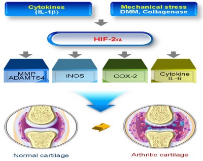
Cause of Osteoarthritis Discovered The fundamental cause of osteoarthritis, a puzzle that had thus far proven elusive to resolve, has been identified by Korean researchers. A research team led by life science professor Chun Jang-soo at the Gwangju Institute of Science and Technology has resolved the puzzle of osteoarthritis with support from the Leading Research Center Assistance Program, conducted by the Ministry of Education, Science and Technology(Ahn Byung-man, Minister), and the Korea Research Foundation (Park Chan-mo, Chairman). The team discovered that the HIF- gene regulates diverse factors that cause degeneration of cartilage cells and spur the disease's development. Hypoxia-inducible factor- is a protein that was known first as a transcription factor whose protein volume increases due to hypoxia. In this study, this protein has been found, apart from previously known functions, to regulate the emergence of diverse genes that are involved in osteoarthritis. Osteoarthritis is characterized by cartilage tissue that gradually wears down and fails to recover due to inherent factors, including aging and heredity, or mechanical factors, such as damage or obesity. According to studies, eight out of 10 elderly citizens aged 65 or older in Korea suffer from the disease. However, the cause and treatment of the condition had not been discovered thus far. HIF- is excessively expressed in cartilage tissue due to DMM (ligament surgery), as well as mechanical stress resulting from the injection of 'collagenase,' or inflammatory cytokine (IL-, etc). HIF- induces osteoarthritis by regulating the emergence of factors that cause cartilage degeneration as transcription factors, or factors including MMP1, 3, 9, 12, and 13 and ADAMTS4, which dissolve cartilage matrix, as well as the expression of genes that cause inflammation such as iNOS and COX-2. MMP (matrix metalloproteinase)This is an enzyme protein that dissolves extracellular matrix; more than 20 types of this protein exist. If these enzymes are activated in the course of cartilage destruction, cartilage matrix molecules are dissolved, inducing regenerative arthritis.ADAMTS (matrix metalloproteinase)Among the extracellular matrix that comprises cartilage, ADAMTS(matrix metalloproteinase) is an enzyme that dissolves sulfate proteoglycan; diverse types of the enzyme exist. Notably, ADAMTS-4 and ADAMTS-5 are known to be involved in osteoarthritis. The researchers also found that if HIF- is artificially generated in cartilage of mice or rabbits, it induces severe osteoarthritis; whereas if HIF- is lacking, osteoarthritis does not occur. Thus, the researchers have opened up the possibility for both prevention and treatment of the condition. The photo on the left shows the development of osteoarthritis in a genetically modified mouse in which HIF- is excessively expressed in cartilage; the photo on the right shows the suppression of osteoarthritis in a genetically modified mouse, which lacks HIF-. Explaining the significance of his study The study will be published as a notable paper in the latest issue of Nature Medicine, the academic journal on basic biomedical science. Lim Dong-Wookduim at kofac.or.kr [June 15, 2010] - - - - - - -Source - ScienceTimes -
042011. 10
No. 58 View. 25383
Scientist Resolve Decade-long Puzzle of 'Protein Function'
Scientist Resolve Decade-long Puzzle of 'Protein Function' The Ministry of Education, Science and Technology(Ahn Byung-man, Minister) said on May 7 that a research team led mostly by Korean researchers had identified for the first time that Synaptotagmin1, a plasma membrane protein, proactively regulates the communication processes of nerve cells. Study published in world's top journal, Science Synaptotagmin1 is one of two major proteins that regulate the excretion of neurotransmitters. Thus far, the research community has speculated that simple introduction of calcium ions leads Synaptotagmin1 to excrete neurotransmitters, but has failed to identify its exact functions. In the study led by Prof. Yoon Tae-young of KAIST, the researchers identified that Synaptotagmin1 serves as a switch that freely regulates the intensity of communication between nerve cells. The research team confirmed for the first time that the introduction of calcium ions at an appropriate density level(10umol/L) into nerve cells causes Synaptotagmin1 to swiftly excrete neurotransmitters, but that contrary to expectations, their introduction at above the appropriate density level decreases the function. This indicates that Synaptotagmin1 responds in various fashions according to the density of calcium emitted from nerve cells. Thus, the scientists have newly discovered that Synaptotagmin1 can freely control the intensity of communication between nerve cells. The new study has discovered for the first time that Synaptotagmin1 most robustly activates at a low calcium density level, and precisely explained the function of Synaptotagmin1, a puzzle that previous studies had failed to resolve. The research team also identified that the detachment of Synaptotagmin1 from membranes leads to the loss of its regulatory switching function, thus discovering that the attachment and non-attachment of Synaptotagmin1 onto and from membrane comprise the centerpiece of its function. Furthermore, Prof. Yoon's research team successfully developed a new technology that allows scientists to monitor the functions of membrane proteins, which are a major target in the quest to develop next-generation new drugs. According to the ministry, membrane proteins play essential roles within the cell, including substance transport, and are closely related with diverse diseases, including cancer, diabetes, and obesity. Hence, they account for up to nearly 70% of the target proteins in the effort to develop new next-generation drugs. The team successfully developed single-vesicle fluorescence detection, and thus secured internationally top-flight technology that allows them to monitor the function of membrane proteins at single-molecule or multi-molecule levels. Prof. Yoon said, "The study has identified the function of Synaptotagmin1, which the academic community has failed to decipher over the past 10 years, and has developed a new technology that enables us to monitor the complicated functions of membrane proteins at the molecular level." Expounding on the significance of his research, he added, "The study has tapped the possibility to develop new drugs for diseases afflicting people of the modern world, including cancer, diabetes and obesity." The study was conducted jointly by nine researchers, including Prof. Yoon, Dr. Lee Han-ki of POSTECH, Prof. Shin Yeon-kyun of Iowa State University, Prof. Kweon Dae-hyuk of Sungkyunkwan University, and Prof. Hyeon Chang-bong of the Korea Institute of Advanced Study. The study was published in the May 7 issue of Science, one of the world's top science journals. [May 31, 2010] - - - - - - -Source - HelloDD.com -
042011. 10
No. 57 View. 26616
New Fundamental Technology Increases Light Extraction Efficiency by 30%
New Fundamental Technology Increases Light Extraction Efficiency by 30% A Korean research team has opened up the possibility to preoccupy the global LED lighting market. The Ministry of Education, Science and Technology(Ahn Byung-man, Minister) said a Korean research team had developed a fundamental technology that increases the light extraction efficiency of InGaN green LED, a next-generation lighting source, by more than 30%. Korean researchers increase green LED's efficiency to carve out global lighting market Indium Gallium Nitride (InGaN)Materials essential for forming active layers for white, blue, green, ultraviolet-ray LED The study, which was led by Prof. Jung Gun-young from the department of new materials engineering at the Gwangju Institute of Science and Technology, and senior researcher Jeong Mun-seok of GIST's Advanced Photonics Research Institute. The study was conducted with support from the Basic Science Research Program and the Nano R&D Program, which are operated by the Ministry of Education, Science and Technology and the Korea Research Foundation. The study was published as 'frontispiece' in the April 9 issue of Advanced Functional Materials. LED, a next-generation lighting source, is a green energy technology that is highly sought after because of its high energy efficiency and eco-friendliness. Unlike conventional lighting such as light bulbs and florescent lights, LED technology presents high efficiency in the conversion of electric energy into light energy, and thus helps cut energy consumption by up to 90%. If Korea replaces 30% of its lighting needs with LED lighting, the country can cut 16 billion kWh(volume equivalent to power generation volume of two 1 million kW-class nuclear power plants) from its electricity consumption, and effectively reduce 6.8 million tons of carbon dioxide emission. "Aiming to preoccupy US$110 billion market by integrating with subsequent research" The newly developed technology does not degrade the electrical characteristic of LED, when compared with the conventional LED, but rather increases light emitting efficiency by more than 30% through the "photo wave guide" effect in zinc oxide(ZnO) nanorods. The photo wave guide effect refers to a technology that increases LED efficiency by creating a photo wave guide, a route through which light travels, in the LED device. The researchers cultivated ZnO sub-microrods using a hydrothermal method on an ITO top contact layer of InGaN green LED(light emitting diode). Subsequently, the researchers investigated whether ZnO nanorods efficiently absorb and emit light generated from the LED by using a micro microscope they developed on their own. Hydrothermal methodA method of synthesis conducted by melting a reactant in water and heating it up at temperatures below 100 degrees Celsius As a result, the researchers discovered that when LED emits light, light transmitted via ZnO nanorods was efficiently extracted at the tip of the rods. Through this experiment, the research team demonstrated that ZnO nanorods served as a route for light transmission, and thus increased the light emitting efficiency of the LED structure. Prof. Jung Gun-young said, "With the study, we have developed a fundamental technology that drastically increases light emitting efficiency in the aspect of materials costs and processing costs," adding, "If we fuse this technology with the results of our subsequent studies, we expect that Korea will be able to preoccupy the global LED lighting market, which is projected to reach US$ 110 billion in 2015." ? Kim Chung-hanchkim at kofac.or.kr [May 10, 2010] - - - - - - -Source - ScienceTimes -
042011. 10
No. 56 View. 30674
'Hepatitis B Treatment' with Indigenous Natural Plant Developed
Liver disease is the biggest cause of death among people in their 40s and the third-biggest cause among those in their 30s. Hepatitis B infection is a major cause of chronic liver disease, with the virus isolated in 73 percent of patients with chronic hepatitis and cirrhosis, and 77 percent of patients with primary liver cancer. KRIBB Dr. Lee Young-ik seeks 'zero' mutation by utilizing indigenous natural plant. Likewise, patients infected with hepatitis B, if left untreated, are effectively constantly exposed to the risk of developing liver cancer, which is caused by the virus. Many anti viral drugs, including lamivudin and interferon, which are commonly used to treat hepatitis B, are widely available in the market. Interferon temporarily increases immunity, while Lamivdin suppresses the activity of DNA polymerase, and curbs its reproduction, resulting in temporary efficacy of treatment. However, when used for a long period of time, this drug allows for the mutation of hepatitis B virus, rendering it resistant to the treatment, while e-antibody continues to be excreted. As a result, a high portion of hepatitis infection progresses into Liver cirrhosis and liver cancer. For this reason, doctors have had to take the trouble of prescribing alternative treatments to patients, coincidently with the emergence of the mutated virus. Dr. Lee Young-ik at the Korea Institute of Bioscience and Biotechnology(Park Young-hoon, President) developed a treatment that suppresses the cause that triggers different mutations to address the problem. At the start of his research, Dr. Lee set the goal of developing a drug for suppressing the emergence of the mutated virus at the time of the secretion of e-antibodies, the integration of hepatitis B virus and liver cancer, and the reproduction of Polymerase, while retaining the efficacy of conventional treatment. In order to develop a new drug, Lee's team first searched for a material that has a suppressing effect. His effort to develop hepatitis B treatment saw no gain through genetic methods or chemical approaches that he had researched previously. Subsequently, learning by change that certain indigenous plants have efficacy, he began research using such plants in earnest with support from the New Frontier R&D Program Plant Diversity Research Center(Joung Hyouk, Director) from 2006. Dr. Lee singled out 135 plant species, which had been used in treating liver disease since ancient times, from the plant extract bank of the New Frontier R&D Program Plant Diversity Research Center. Of these, he singled out eight plant species that were found to directly remove the hepatitis virus, and finally selected on three indigenous plants, including Phyllanthus Urinaria Koreana. He then extracted virus-suppressing substances from the indigenous plants, developed a treatment and conducted animal tests. The substance effectively lowered the portion of mutations, which stood at as high as 10^6/1 to 10^18/1, which is far superior to conventional treatment. "The most important thing in the development of the treatment is the fact that we have developed substances that suppress mutations at different points in time from the three indigenous plants. Based on these substances, we have developed treatments whose operational mechanisms are completely different from those of conventional anti-viral drugs." His study is currently undergoing tests for safety and efficacy. In particular, noting that the hepatic B virus in pregnant women can be transmitted to the fetus, he injected the new treatment into cubs given birth by animals with the virus, and is conducting experiments to determine how the treatment affects the cubs with the virus. Dr. Lee said, "Considering the results of efficacy tests and the development process thus far, we anticipate positive findings from the safety evaluation process," adding, "When we finish animal tests, we will begin a process for the treatment's commercialization in earnest in accordance with the rules and regulation of the Korea Food and Drug Administration." Dr. Lee, who has researched viruses for more than 20 years, aims to develop treatments for Cirrhosis and liver cancer, on top of treatments for hepatitis B. "Since the liver is a central organ of humans, I would like to concurrently study metabolic diseases as well. Just as we were able to generate promising research with support from the New Frontier R&D Program Plant Diversity Research Center, I hope that well-organized research support programs with similar purposes can provide ample assistance to researchers." Kim Hee-jin [April 26, 2010] - - - - - - -Source - HelloDD.com -
042011. 10
No. 55 View. 25748
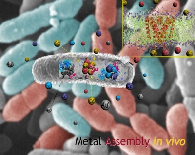
New Process for Synthesizing Metal Nanoparticles Developed
Korean researchers have developed a new process that allows for synthesis of metal nanoparticles of diverse sizes and kinds through a novel bioengineering method. 'New technology to allow for creation of metal nanoparticles using microorganisms' Prof. Lee Sang-yup and research professor Kim Tae-jung of KAIST(Suh Nam-pyo, President) said on September 1 that they had developed a technology that allows for the production of quantum dots and magnetic nanoparticles, and metal nanoparticles of diverse types, which had previously not been synthesized, by regulating the secretion of heavy metal-absorbing protein in E-coli and peptides; the technology also allows for free control of the size of metal nanoparticles by adjusting the density of metallic ions that are added in the process. The study was published on August 18 in the online edition of Angewandte Chemie International Edition, a world-renowned chemistry journal, and was introduced as a "hot paper," earning recognition for its significance. Prof. Lee Sang-yup and research professor Kim Tae-jung The researchers excreted metallothionein, a protein that binds with metallic ions, and phytochelatin, a peptide, either independently or through combinations in E-coli, and exposed diverse metallic ions to the cultured fluid, thus generating diverse metal nanoparticles. By regulating the excretion of metal-binding protein, and the density of metallic ions, the researchers generated quantum dot, nano-magnet, and gold nanoparticles of diverse sizes, as well as metal particles that had never before been chemically synthesized. If recombinant E-coli cells are separated through centrifugation and crushed, thus removing various organic substances, only the synthesized metal nanoparticles can be acquired easily. By attaching diverse bioactive materials to the surface of these metal nanoparticles, the researchers presented the possibility of using biologically synthesized nanoparticles for research on various drug delivery systems and developing medical diagnostic tools that use animal cells. Prof. Lee said, "The study presented a technology that allows for efficient and convenient synthesis of desirable nanoparticles through biotechnological culturing of recombinant microorganisms instead of the conventional physical and chemical process," adding, "The technology will have diverse applications in medicine and bioengineering research in the future." The study was conducted with support from the World Class University program, which is operated by the Ministry of Education, Science and Technology(Lee Ju-ho, Minister) and the Korea Research Foundation(Park Chan-mo, Chairman), and from the "Industrial Fusion Technology, Industrial Core Technology Development Program" sponsored by the Ministry of Knowledge Economy(Choi Kyung-hwan, Minister). Kim Josephjoesmy at HelloDD.com twitter: at ssebiU [September 27, 2010] - - - - - - -Source - HelloDD.com